Why DC/DC Converters Fail EMC — and How to Fix It
- Reto Keller

- Feb 8
- 7 min read
DC/DC converters are a common cause of failed CISPR 11 and CISPR 32 EMC emission tests. This blog shares practical PCB layout techniques that help you pass EMC emissions tests.

1. Introduction
Based on personal experience, the following are some of the most important considerations for reducing emissions from DCDC-converter circuits:
Use a multilayer PCB with a solid ground (GND) plane.
Minimize the size of critical current branches.
Reduce coupling from the switching node to the feedback path and output.
2. Use Multilayer PCB With Solid GND Plane
Using a multilayer PCB with a solid ground (GND) plane is a cost-effective way to reduce both conducted and radiated emissions in DC/DC converter PCB designs. The GND plane should be placed directly adjacent to the DC/DC converter signals — so that there is a solid GND plane immediately beneath the converter circuit. This plane helps to minimize the inductance for currents with fast transients (high di/dt [A/s]) and, as a result, reduces unintended magnetic H-fields [A/m] (compare Figure 1 and Figure 2).
Note: Do not split or cut the ground plane beneath the DC/DC converter circuit. Instead, use a solid GND plane, which most effectively minimizes the loop areas of critical current paths.


The critical current branches are those with high di/dt [A/sec]. The branches containing the switch and the diode are always critical, because the current through the switch and diode can change from several amperes to 0 A in just a few nanoseconds. The next section describes this in more detail.

3. Minimize The Size Of Critical Current Loops
3.1 What Are Critical Current Branches?
Figure 4 shows the forward and return currents of a simplified buck converter DC/DC circuit schematic. Critical current branches are branches of DC/DC converter circuits with a high di/dt [A/sec] and no mirror current. A mirror (return) current in such a case means a current that is identical to the forward current, but in the opposite direction. Current branches with high di/dt [A/sec] and without mirror current increase the possibility of noise voltage vn(t) [V] induction in nearby current loops. If we assume a circuit 1 (the noise source) with a current change of di1/dt and a circuit 2 (the victim) with a mutual inductance M12 [H] of these two circuits, the induced noise voltage vn(t) [V] in circuit 2 can be calculated as [1]:

The equation above shows that the higher di/dt [A/sec], the larger the noise voltage vn(t).

A mirror current is a current that is identical to the forward current but in the opposite direction. For DC/DC converter current branches of Figure 4, we can distinguish between these two cases:
a. There is a mirror current
b. There is no mirror current
In case a.), there is the chance that the magnetic H-field [A/m] of the forward current can be minimized out by routing the mirror return current very close to the forward current, e.g. by enabling it to flow in a directly adjacent GND plane (see Figure 1).
In case b.), there is no nearby mirror current and therefore the H-field [A/m] of the current is not “canceled out” (see Figure 2), and due to its high di/dt [A/sec], the possibility of inducing noise voltage in nearby current loops is higher than in case a.).
3.2 How To Identify Critical Current Branches?
How can we identify the critical current branches in a DC/DC converter PCB design? We go through this with an example of a buck converter, which converts a higher DC voltage (Vin [V]) to a smaller DC voltage (Vout [V]).

Let’s have a look at Figure 5. It shows the principal schematic of a DC/DC buck converter. Vsupply [V] is the input power supply, and Cin [F] is the input filter of the actual DC/DC converter circuit. The P-channel MOSFET presents the switch, and D is the diode of the DC/DC converter circuit. L [H] represents the inductance of the DC/DC converter, and Cout [F] is the output filter. Rload [Ω] stands for any load circuit.
Figure 6 shows the current flow in the DC/DC buck converter design when the DC/DC converter switch is closed, and Figure 7 shows the current flow when the switch is open.

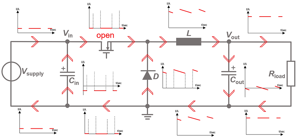
Figure 8 shows the current flow when the switch opens and closes consecutively, and helps us to identify the critical current branches. The most critical current branches are the branches that don’t have a mirror current and have high di/dt [A/sec].

3.3 Critical Current Loops Of Buck, Boost and Buck-Boost Converters
For the sake of simplicity, electronic and PCB designers often talk about the “critical current loops” and not about “critical current branches”. These “critical current loops” are not bound to a current source and load in the classical way. The “critical current loops” just contain the branches that are considered the most critical in terms of EMC. Such critical “current loops” are shown in Figure 9 for a simplified DC/DC buck converter example.

Figure 10 shows the critical current loops for DC/DC buck, boost, and buck-boost converter designs. The area of these current loops should be minimized for low conducted and radiated emissions and to meet the EMC emissions limits defined by CISPR 11 and CISPR 32. The minimization of the current loop areas leads to a lower mutual inductance M12 [H] between the victim and the noise circuit (see formula for the inductive noise coupling in the previous section) and can be achieved:
with a solid GND plane underneath the DC/DC converter circuit on a PCB and,
by placing the filter capacitors Cin [F] and Cout [F], the diode D, and the inductor L accordingly.

3.3 Minimize Coupling From Switching Node
The switching nodes of DC/DC converter designs have very high dv/dt [V/sec]. Figure 11 shows what is generally meant by the term “switching node” (in yellow). As high dv/dt [V/sec] increases the probability of capacitive (near-field) noise coupling into circuits, traces, and components nearby, this high dv/dt [A/sec] node should be kept small and away from sensitive signals.

The voltage on the switching node can change from several volts to 0V within a couple of nanoseconds, which leads to slew-rates of up to >100kV/sec. This means that this node could potentially introduce significant noise currents in(t) [A] in nearby circuits, via capacitive coupling:

where in is the coupled noise current into the victim circuit in [A], Cstray is the (stray) coupling capacitance between the switching node and the victim circuit in [F], and dv/dt is the slew-rate of the switching node signal.
Note: High impedance circuits are more sensitive to capacitive coupling – like the feedback signal of DC/DC converters – than low impedance circuits.
4. PCBA Layout Examples For DC/DC Buck Converter
The feedback signal is the most sensitive signal of a DC/DC converter circuit, and the feedback input (FB) of the DC/DC converter chip is usually of high impedance (sensitive to capacitive coupling). Therefore, the feedback signal should be routed with care and away from the switching node (high dv/dt [V/sec]). A good and a bad case of the feedback signal routing is shown in Figure 12.
Moreover, placing Cin [F] close to Vin of the DC/DC converter chip helps to minimize the high di/dt [A/sec] current loop area in a buck converter design (see Figure 12).
In addition, it is important that the input filter capacitor (Cin [F]) and the output filter capacitor (Cout [F]) have their own low-inductance connection to the solid ground plane on the 2nd layer (e.g., with two separate vias like shown in Figure 12).
In case of high output currents (e.g. >10A) Monolithic Power Systems (MPS) recommends that the feedback voltage divider resistors (R1, R2) are not connected to the ground/power planes but rather apply the concept of – what MPS calls – “remote sampling”. In the case of “remote sampling”, the voltage feedback divider resistors (R1, R2) are connected with dedicated PCB traces to Cout (and not with GND- and power-plane-vias) [3]. This concept is applied and shown in Figure 12 (good example).

5. Conclusion
This blog presented simple concepts for DC/DC converter PCB designs that can be applied universally to meet the EMC emission requirements of CISPR 11 or CISPR 32. To summarize this blog post in one sentence:
“Use a solid GND plane underneath the DC/DC converter circuit, place DC/DC converter components in a way that the critical current branches (with high di/dt [A/sec]) are kept short and reduce the copper area of the switching node (very high dv/dt [V/sec]), while increasing the distance between the switching node copper area and other traces and components.”
Here is a checklist for your next DC/DC converter design:
☐ Use a multi-layer PCB with a solid ground plane beneath the DC/DC converter circuit
☐ Keep branches with high di/dt [A/sec] as short.
☐ Keep the switching node copper area small.
☐ Keep the feedback signal away from the switching node copper area.
☐ Place (at least) two separate ground vias for each filter capacitor Cin and Cout.
About The Author
Reto Keller is a principal electronic development engineer and is currently president of the Academy of EMC. Furthermore, he is a committee member of the IEC TC 65/SC 65A/WG4 (EMC standard IEC 61326-2-6).

References
[1] Henry W. Ott. Electromagnetic Compatibility Engineering. John Wiley & Sons Inc., Sept. 11, 2009
[2] Sanjaya Maniktala. Switching Power Supplies A-Z. Newnes, 2nd edition, 2012.
[3] Monolithic Power Systems. Designing the Feedback Voltage Resistor Divider in a DC/DC Converter. https://www.monolithicpower.com/learning/resources/designing-the-feedback-voltage-resistor-divider-in-a-DC/DC-converter [2026-Jan-10].


The fit and overall design of this hoodie look really on point. It’s not too flashy but still has enough personality to stand out. I’ve seen similar styles on the Giggly Squad streetwear hoodies shop, which focuses on clean and modern looks.
I found this explanation of why DC‑DC converters fail EMC very clear and practical. It’s great how you break down common issues and offer real fixes that engineers can try. I’ve been learning more about electronics while juggling studies, and sometimes I depend on a US online class taker to help manage my workload. Posts like this make complex topics easier to understand and apply.